| OVERVIEW
This is a simple design tool for calculating bias resistor values,
small-signal gain and input/output resistances of a common-source JFET amplifier.
Just fill the input fields below in given order from top to bottom.
The ordering of the fields serves as a step-by-step guide for the design process.
The resistor values are calculated automatically using 5% tolerance resistances.
The biasing will be set by choosing the desired gate-to-source voltage Vgs.
Choosing Vgs = Vp/2 implies a middle-bias and values close to Vp will give
more gain and increase output impedance.
Note to keep enough headroom for the input signal when choosing the operating point of Vgs.
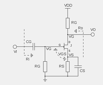
The small-signal values are evaluated in the mid-band, CG and CS short-circuited (source resistor bypass).
The small-signal gain is evaluated as VO/VI, and the input/output
resistances are evaluated as shown in the schematic.
Typical characteristic values for a n-type JFET are given as: Idss = 0.005, Vp = -1.8, for example. |
 |
| Select the operating voltage VDD. Typically 9 volts is the way to go. |
VDD : |
volts |
RESULTS
DC Bias voltages:
VD : volts
VS : volts
VG : volts
Drain resistor:
RD : ohms
Source resistor:
RS : ohms
AC Gain factor:
Av : const
Input resistance:
Ri : ohms
Output resistance:
Ro : ohms
|
| Measure the saturation current Idss of the device by connecting source and gate to ground
and placing a 10 ohm resistor between drain and Vdd.
Use a multimeter to measure the voltage drop over the resistor and use Ohm's law to convert the measured voltage into current.
Alternatively, select a typical value of Idss from the datasheet. |
Idss : |
amps |
| Measure the pinch-off voltage Vp of the device by connecting gate to ground, drain to Vdd and
a 1 megohm resistor between source and ground.
Use a multimeter to measure the voltage drop over the resistor.
The voltage drop is quite close to Vp.
Alternatively, select a typical value of Vp from the datasheet. |
Vp : |
volts |
| Choose the gate-to-source bias voltage Vgs.
Select Vgs = Vp/2 if not sure.
Values closer to Vp will give larger drain and source resistor values, increase gain
and bring the drain bias voltage closer to VDD/2. |
VGS : |
volts |
| Choose the gate resistance RG.
This resistance value will determine the input impedance Ri of the amplifier configuration |
RG : |
ohms |
| For gain analysis, the internal output resistance of the JFET device is needed.
This is usually found from the datasheet as output admittance Yos,
where the output resistance is the inverse, rd = 1/Yos. |
rd : |
ohms |
|